IIT Guwahati and Tata Electronics have signed an MoU to establish a Centre of Excellence focused on semiconductor education, practical training and research.
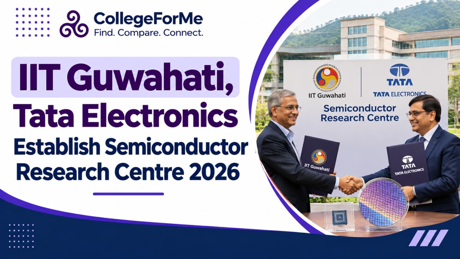
The Indian Institute of Technology (IIT) Guwahati has signed a Memorandum of Understanding (MoU) with Tata Electronics Private Limited to strengthen semiconductor education, technical skill development and research in India. Under this collaboration, both organisations will establish a Centre of Excellence (CoE) at the IIT Guwahati campus, focusing on semiconductor Assembly, Testing, Marking and Packaging (ATMP).
The initiative aims to develop industry-ready professionals by connecting academic education with practical industry requirements. It will introduce diploma-level training and BTech-level engineering programmes in semiconductor ATMP, along with hands-on learning opportunities.
The collaboration will also extend educational opportunities to students from engineering colleges, polytechnics and other educational institutions across Assam and the Northeast region. Undergraduate and postgraduate students will also get opportunities to participate in collaborative research activities.
Students interested in engineering courses can also explore the guide on College For Me to understand different engineering institutions and academic opportunities.
The collaboration was announced on October 30, 2026, and focuses on connecting academic education with the growing requirements of India's semiconductor industry.
IIT Guwahati and Tata Electronics Collaboration: Key Highlights
The partnership focuses on building a strong semiconductor education and research ecosystem through academic and industrial collaboration.
Here are the major highlights of this initiative:
Centre of Excellence: A dedicated semiconductor Centre of Excellence will be established at IIT Guwahati.
Diploma-Level Training: Specialised training programmes will be developed for students interested in semiconductor technologies.
BTech-Level Programmes: Engineering programmes will focus on semiconductor Assembly, Testing, Marking and Packaging.
Practical Learning: Students will get hands-on training opportunities.
Industry Exposure: Students will have opportunities for training at Tata Electronics.
Research Opportunities: Undergraduate and postgraduate students will be able to participate in collaborative research projects.
Faculty Development: Faculty members from participating institutions will receive specialised training.
Regional Education: Engineering colleges, universities and polytechnics across Assam and the Northeast will be identified for participation.
What Is the Semiconductor Centre of Excellence at IIT Guwahati?
The Centre of Excellence (CoE) will be established at the IIT Guwahati campus to support specialised semiconductor education, technical training and research.
The centre will act as a hub for developing industry-oriented educational programmes and research activities in semiconductor packaging technologies.
IIT Guwahati will lead the development and delivery of educational programmes, while Tata Electronics will contribute industry expertise to develop relevant course content and specialised training modules.
The main objective is to reduce the gap between theoretical engineering education and the practical skills required in the semiconductor industry.
Role of IIT Guwahati
IIT Guwahati will take responsibility for developing and delivering academic and training programmes.
The institute will focus on diploma-level training and BTech-level engineering programmes in semiconductor ATMP. It will also identify engineering colleges, universities and polytechnics that can participate in this initiative.
Additionally, IIT Guwahati will support academic research and faculty development activities related to semiconductor technologies.
Students can also explore Engineering Career Counselling at College For Me to learn about engineering branches, college options and possible career pathways.
Role of Tata Electronics
Tata Electronics will contribute industry knowledge and expertise to the collaboration.
The company will work with IIT Guwahati to develop industry-relevant course content, specialised training programmes and educational resources.
Students will also get opportunities for practical training at Tata Electronics, helping them understand how semiconductor-related processes are applied in an industrial environment.
What Is Semiconductor ATMP Technology?
ATMP stands for Assembly, Testing, Marking and Packaging. It is an important part of semiconductor manufacturing that focuses on preparing fabricated semiconductor chips for use in electronic devices.
After a semiconductor chip is fabricated, it goes through several processes to ensure that it is properly assembled, tested, identified and protected.
The four major stages of ATMP are explained below.
1. Assembly
Assembly involves connecting semiconductor chips with the required components and structures.
Students can develop an understanding of chip assembly concepts, component integration and the importance of proper connections in semiconductor devices.
2. Testing
Testing is performed to check whether semiconductor chips are functioning correctly and meeting the required performance standards.
Students can understand the importance of testing, identifying defects and checking the reliability of semiconductor components.
3. Marking
Marking involves adding identification information to semiconductor components.
It helps in identifying and tracking semiconductor products during manufacturing and related processes.
4. Packaging
Packaging protects semiconductor chips and provides the necessary electrical connections for their use in electronic devices.
Students can learn about packaging concepts, chip protection, electrical connections and the importance of packaging in semiconductor technology.
What Will Engineering Students Learn Through This Collaboration?
One of the most important aspects of this partnership is its focus on practical semiconductor education.
The programmes will combine classroom learning with hands-on training to help students understand semiconductor packaging technologies and their industrial applications.
Students interested in electronics, electrical engineering, computer science and related technical fields may find these learning areas relevant.
1. Fundamentals of Semiconductor Technology
Students will have an opportunity to develop an understanding of semiconductor technology and its importance in modern electronics.
They can build knowledge about:
What semiconductors are and how they are used.
Basic concepts of semiconductor chips.
The role of semiconductor components in electronic devices.
Basic properties of semiconductor materials.
Applications of semiconductor technology in computers, smartphones, automobiles and communication systems.
2. Semiconductor Assembly and Packaging
Assembly and packaging are important areas of semiconductor ATMP.
Students can learn about:
Basic semiconductor chip assembly concepts.
Different packaging concepts and their applications.
How semiconductor chips are connected with electronic components.
The importance of chip protection.
How packaging supports the performance and reliability of semiconductor devices.
3. Semiconductor Testing and Quality Checking
Testing is essential for checking the functionality and quality of semiconductor components.
Students can develop an understanding of:
Why semiconductor testing is required.
Basic concepts of testing electronic components.
Identifying defects in semiconductor products.
Understanding product quality and reliability.
The importance of quality checking in semiconductor manufacturing.
4. Practical and Hands-On Technical Skills
The collaboration specifically includes hands-on training as part of the educational programmes.
Students will get opportunities to connect classroom concepts with practical applications.
The learning experience is expected to help students understand:
Practical semiconductor ATMP processes.
How theoretical concepts are applied in industrial environments.
The importance of technical accuracy.
Semiconductor packaging and testing workflows.
Industry-oriented technical practices.
The exact practical modules and equipment will depend on the detailed programme curriculum.
5. Industry-Oriented Technical Knowledge
Another important objective is to prepare students according to the requirements of the semiconductor industry.
IIT Guwahati and Tata Electronics will jointly develop industry-relevant course content and specialised training resources.
Students can benefit from understanding:
Industrial semiconductor processes.
Technical requirements of semiconductor packaging.
The connection between academic learning and manufacturing.
Industry practices related to assembly and testing.
The importance of quality and technical skills in semiconductor operations.
6. Research and Problem-Solving Skills
The collaboration will also provide research opportunities to undergraduate and postgraduate students.
Students can develop their understanding of semiconductor packaging, assembly, testing and related technologies through collaborative research activities.
Research-based learning can help students improve:
Technical problem-solving.
Research and analytical thinking.
Understanding of semiconductor technologies.
Technical documentation and project work.
Innovation and experimentation.
How Will Students Benefit from IIT Guwahati and Tata Electronics Collaboration?
This partnership can provide several academic and professional learning benefits to engineering students.
1. Access to Specialised Semiconductor Education
Students will get opportunities to learn about semiconductor technologies through specialised diploma-level and BTech-level educational programmes.
2. Practical Training Opportunities
The programmes will include hands-on training to help students understand how semiconductor concepts are applied in practical situations.
3. Industry Exposure at Tata Electronics
Students will have opportunities for training at Tata Electronics. This can help them understand industrial working environments, technical processes and semiconductor-related operations.
4. Better Understanding of Semiconductor Manufacturing
Students will get exposure to important areas such as assembly, testing, marking and packaging.
5. Collaborative Research Opportunities
Undergraduate and postgraduate students will be able to participate in collaborative research activities and explore advanced semiconductor technologies.
6. Faculty Training and Improved Learning Resources
Faculty members from participating educational institutions will receive specialised training to strengthen semiconductor-related teaching capabilities.
7. Opportunities for Students Across Northeast India
The initiative will identify engineering colleges, universities and polytechnics across Assam and the Northeast region, expanding access to specialised technical education.
Students looking for additional engineering education guidance can also read Best BTech Colleges in Delhi NCR 2026 on College For Me.
What Career Opportunities Can Students Explore After Learning Semiconductor Technology?
The semiconductor industry includes several technical areas related to chip packaging, assembly, testing, electronics and research.
Students who develop relevant technical knowledge and practical skills may explore different career pathways depending on their qualifications, specialisation and experience.
1. Semiconductor Packaging Engineer
Packaging engineers work on processes involved in protecting semiconductor chips and preparing them for use in electronic devices.
2. Semiconductor Testing Engineer
Testing engineers check the performance, functionality and quality of semiconductor components.
3. Process Engineer
Process engineers work on improving and monitoring technical processes used in semiconductor manufacturing and packaging operations.
4. Quality Control Engineer
Quality control professionals focus on checking product quality, identifying defects and maintaining manufacturing standards.
5. Semiconductor Research Professional
Students interested in higher education and research can explore advanced studies and research activities in semiconductor materials, packaging and related technologies.
6. Electronics and Manufacturing Engineer
Students with relevant engineering knowledge can also explore technical roles related to electronics manufacturing and industrial operations.
These are possible career areas associated with semiconductor technologies, not confirmed placement roles or job guarantees under this collaboration.
Why Is This Initiative Important for India's Semiconductor Industry?
Semiconductors are essential components of modern electronic devices, including smartphones, computers, automobiles, medical equipment and communication systems.
As the demand for electronic products increases, the need for skilled semiconductor professionals also becomes important.
India is working towards strengthening its semiconductor ecosystem through investments, research, technical education and industry collaborations.
The partnership between IIT Guwahati and Tata Electronics supports this development by connecting academic institutions with industry expertise.
The initiative is particularly relevant for Assam and the Northeast region because it aims to expand specialised technical education beyond a single institute.
By introducing industry-oriented programmes, practical training and collaborative research, the partnership can contribute to developing a skilled workforce for India's semiconductor sector.
ALSO READ
1.
https://www.collegeforme.in/counselling
2. https://www.collegeforme.in/colleges
3. https://www.collegeforme.in/exams
Frequently Asked Questions (FAQs)
1. What is the collaboration between IIT Guwahati and Tata Electronics?
IIT Guwahati and Tata Electronics have signed a Memorandum of Understanding to establish a Centre of Excellence focused on semiconductor education, skill development and research.
2. When was the IIT Guwahati and Tata Electronics collaboration announced?
The collaboration was officially announced on October 30, 2026.
3. What is the main objective of the semiconductor Centre of Excellence?
The main objective is to develop skilled professionals through specialised education, practical training and research in semiconductor packaging technologies.
4. What does ATMP stand for in semiconductor manufacturing?
ATMP stands for Assembly, Testing, Marking and Packaging. These processes prepare semiconductor chips for use in electronic devices.
5. What will students learn through this semiconductor initiative?
Students will get opportunities to learn about semiconductor ATMP, chip assembly, packaging, testing, industry-oriented technical concepts and related research activities.
6. Will students receive practical training through this collaboration?
Yes, the planned educational programmes will include hands-on training as part of their curriculum.
7. Will students get training opportunities at Tata Electronics?
Yes, the collaboration includes training opportunities for students at Tata Electronics.
8. Will IIT Guwahati introduce diploma-level and BTech-level programmes?
Yes, the partnership includes plans to develop diploma-level training and BTech-level engineering programmes focused on semiconductor ATMP.
9. Why is the IIT Guwahati and Tata Electronics partnership important for engineering students?
It aims to provide specialised semiconductor education, hands-on training, industry exposure and research opportunities, helping students understand a growing area of engineering and technology.
Conclusion
The collaboration between IIT Guwahati and Tata Electronics is an important development for semiconductor education, technical training and research in India.
Through the proposed Centre of Excellence, students will get opportunities to develop knowledge in semiconductor Assembly, Testing, Marking and Packaging. The planned diploma-level and BTech-level programmes will combine academic learning with practical training and industry exposure.
Students will also have opportunities for training at Tata Electronics and collaborative research in semiconductor packaging and related technologies.
For engineering students interested in electronics, semiconductor manufacturing and advanced technology, this initiative represents an opportunity to explore a specialised technical field and understand its growing importance in India's technology ecosystem.
Topics
Aditya Rai
An education enthusiast dedicated to helping students navigate their academic journey. Writing about colleges, courses, career paths, and everything to help you make informed decisions about your future.
Need help choosing the right college?
Talk to our verified counsellors — completely free. Get personalised guidance for JEE, NEET, CAT & more.
Book Free Counselling SessionComments
- Centre of Excellence: A dedicated semiconductor Centre of Excellence will be established at IIT Guwahati.
- Diploma-Level Training: Specialised training programmes will be developed for students interested in semiconductor technologies.
- BTech-Level Programmes: Engineering programmes will focus on semiconductor Assembly, Testing, Marking and Packaging.
- Practical Learning: Students will get hands-on training opportunities.
- Industry Exposure: Students will have opportunities for training at Tata Electronics.
- Research Opportunities: Undergraduate and postgraduate students will be able to participate in collaborative research projects.